Engineers at FAU develop new scanning method for digital image sensors

A trick with pixels results in sharper images
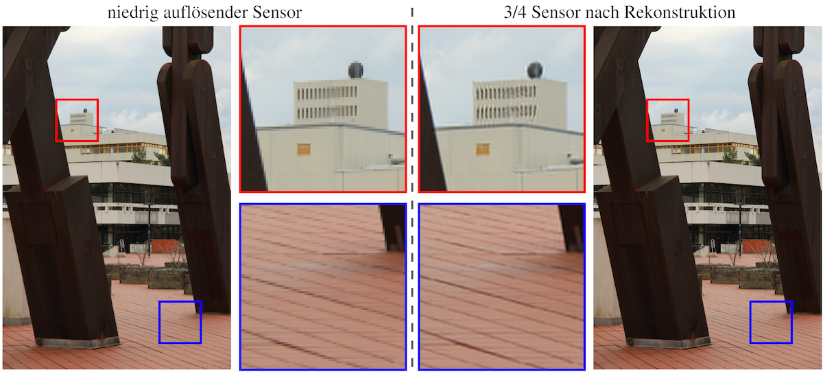
Engineers at FAU have developed a method for increasing the resolution of digital cameras by four times without having to use larger and more expensive image sensors. This is achieved by irregularly scanning the pixels and reconstructing the image afterwards. The next step involves developing a prototype that will enable more research to be carried out.
Everyone who has a smartphone also has a camera. Or to put it more precisely, a digital camera. Its main component is an image sensor that converts the incoming light into a digital signal. To do so, the sensor is split into small sectors called pixels that measure the intensity of the light. Until now, virtually the only way to improve the resolution of a camera (the ability to render more detailed images) was to increase the number of pixels. ‘Using larger or more expensive sensors or scaling down pixels to achieve this is only technically possible to a certain extent,’ says Dr. Jürgen Seiler from the Chair of Multimedia Communications and Signal Processing at FAU. ‘We also have to bear in mind that smaller pixels lead to greater disturbance, or ‘noise’ in the image.’

Regular arrangement leads to aliasing
But how can you improve the resolution of image sensors without having to increase the number of pixels? Seiler and his team have been working on this problem for several years. In contrast to conventional methods where pixels are scanned in a regular manner, their approach involves irregular scanning. ‘Every pixel has an area that is sensitive to light, but also areas where no light is detected’, explains Jürgen Seiler. ‘In conventional sensors, all pixels are evenly arranged in a grid, which leads to severe aliasing artefacts.’ Aliasing causes stepped edges of light or distorted patterns in periodic image contents. This is visible, for example, when a television presenter wears a jacket with a fine checked pattern and when the pattern suddenly turns into colourful blotches.
Four-fold increase in resolution due to rotated image areas
FAU researchers have now been able to demonstrate that aliasing can be reduced effectively by using irregular scanning. To do so they used a trick. The square pixels are still arranged in a regular grid, but they are rotated in opposite directions so that the light-sensitive areas do not line up exactly. ‘You could compare it to tiling a wall with tiles that have a decorative border on them’, says Jürgen Seiler. ‘If each tile is turned by 90 degrees, the border forms an irregular pattern instead of a continuous line.’ The image is reconstructed using a downstream process that was developed at the Chair. With this method, the engineers have increased the resolution that is achieved by regular scanning by a factor of four, while retaining the same number of pixels. This is possible due to the fact that image signals can typically be described by a small number of dominant frequencies, an effect that is also used when compressing audio files.
Prototype for further research
The combination of irregular scanning and downstream processing means that either significantly higher image quality can be achieved with the same number of pixels or the number of pixels can be reduced by a factor of four for the same image quality. With this solution, manufacturers of digital cameras can not only save costs, but also significantly reduce the energy consumption of their devices. The method is still in the simulation phase, however, plans for a prototype that will enable further measurements to be made are in the pipeline.
Further information:
Dr. Jürgen Seiler
Phone: +49 9131 8527102
juergen.seiler@fau.de